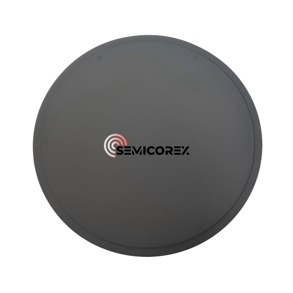
SiC Epitaxy: Building the Future of Power Electronics
2025-04-17
In the world of advanced semiconductors, silicon carbide, commonly known as SiC, is transforming the landscape of power electronics. At the heart of this revolution lies a critical process known as SiC epitaxy. This method is essential for creating high-performance SiC-based devices that are more efficient, more durable, and better suited for demanding applications.
What Is SiC Epitaxy?
Epitaxy is a process used to grow a crystalline layer on top of a substrate in a highly controlled manner. In the case of SiC epitaxy, this involves depositing a thin layer of silicon carbide onto a SiC substrate. The goal is to form a high-quality, defect-free crystal layer that matches the structure of the underlying material.
This process is typically carried out using chemical vapor deposition, or CVD, at very high temperatures. The result is an epitaxial layer that serves as the foundation for manufacturing high-voltage and high-power electronic devices.
Why SiC Epitaxy Matters
SiC epitaxy is crucial for enabling the superior properties of silicon carbide to be fully utilized. Compared to traditional silicon, SiC has a wider bandgap, higher thermal conductivity, and the ability to operate at much higher voltages and temperatures. These qualities make it ideal for use in electric vehicles, renewable energy systems, industrial motors, and aerospace electronics.
However, to manufacture devices that can withstand such intense conditions, the quality of the SiC material must be extremely high. This is where epitaxy comes in. A well-grown epitaxial layer ensures low defect density, high doping control, and excellent surface uniformity — all essential for creating reliable and efficient power devices.
Applications and Benefits
Devices built on SiC epitaxial layers include MOSFETs, Schottky diodes, and bipolar junction transistors. These components are widely used in power conversion systems where efficiency and compact size are critical. For example, SiC devices help reduce energy loss in electric vehicle inverters and improve the performance of solar inverters and fast-charging stations.
Another major benefit is the ability to operate in harsh environments. SiC-based electronics can function at higher temperatures and voltages than their silicon counterparts, reducing the need for bulky cooling systems and allowing for smaller, lighter designs.
Challenges and Advancements
Despite its advantages, SiC epitaxy is a complex and challenging process. Growing thick, uniform layers with low defect levels requires precise control of temperature, gas flow, and chemical composition. Even minor deviations can impact the performance of the final device.
To address these challenges, researchers and manufacturers are continually improving reactor designs, gas chemistry, and in-situ monitoring techniques. Innovations such as multi-wafer CVD systems and advanced simulation tools are helping to increase yield and reduce production costs, making SiC technology more accessible and scalable.
Conclusion
SiC epitaxy is a foundational technology driving the next generation of power electronics. By enabling the growth of high-quality silicon carbide layers, it paves the way for more efficient, compact, and robust electronic devices. As demand for clean energy, electric vehicles, and high-performance systems continues to grow, SiC epitaxy will play an increasingly vital role in shaping a smarter, more energy-efficient future.


